Making a silicon chip logo
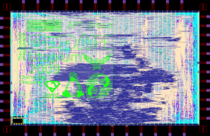
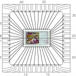 Historically, when manufacturing silicon designs, it used to be a bit of engineering fun to add a little non logo or a cute little image to the design. There are some fantastic examples of this available at Silicon Zoo. Nowadays, it is actually an essential part of the process as a large visible logo makes it easy to spot the different designs on multi project wafers, and is a requirement by the people who do the wire bonding to make sure the chip is correctly oriented. The in-line image is what we send to the people connecting the silicon to the chip package using rather small wires. In the diagram there is the Utopium chip package with a, to-scale, die plot of the silicon with the logo clearly visible and all the wire connections we need. This serves two uses, firstly it shows the orientation of the chip, and secondly it makes sure we don’t have any crossing wires.
This time we are using a reather simple 48 pin DIL package which a rather retro package with relatively few pins, but it makes life easier when making the test board.
Making the Logo
 So, onto making a chip logo. You first need two pieces of information, the minimum top level metal size (in my case the level 8 metal layer for the UMC 130nm process has a minimum width of 1.5um) and the size of the logo (for this example I will make one 0.75mm x 0.6mm). Using those numbers you can determine the size of your canvas (“750um x 600um” / 1.5um is roughly 500 x 400 pixles).
Next, create an image in Gimp (or equivalent) of your required size. Use black on white. Here is our example cat. This now needs to be saved as a .pnm file. When the “Data formatting” dialog pops up, select Ascii. Keep the gimp window open as we will need it later.
Now we need to run pnm2cif on the file. This was written by Andrew Bardsley and is released under the “Whatever you like” licence (GPLv2+ or BSD). Download it to the same directory as the image, and run:
> ./pnm2cif.pl <pnm-image-filename> <cell-name> <scalar> <layer-name>
The pnm file is the image, the cell-name will be the name of the new cell, the scalar is the size of the feature size, and the layer-name is the name of the metal layer used. In our case these are:
> ./pnm2cif.pl cat_logo.pnm cat_logo 1500 ME8
The scalar of 1500 is because the minimum feature size in nanometres, and ME8 is the name of the top level metal layer.
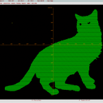 Hopefully this has now produced a .cif file which can be imported into your layout editor. We will use Cadence Virtuoso for this. From ICFB select File -> Import -> CIF, enter the filename and set the Scale UU/DBU to 0.001 micron (the 1nm we used as a base unit) and select the library which it should be imported into. The two warnings are normal. Open up the newly imported cell and make sure it is the correct size.
Because the design is made of metal slices which are not connected we need to merge them all into one. Select all (Ctrl+A) and merge (Shift+M). Now that all the metal slices are merged, the logo is ready to go? Well, no, the design first has to pass the DRC rules.
Passing DRC
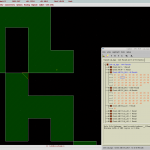 At this stage the design is covered with “Design Rule Check” faults. The most common ones are two pixels meeting at corners, like shown in the in-line image. This essentially creates an infinitely thin wire (the fabrication folk don’t like making these). So, back to gimp, to manually fix these up with a pen. If you tried to use a dithered image, at this point you will be admitting defeat and moving to a simpler design.
![]() The next thing to fix is the maximum wire thickness. This is 30um which is 20 pixels. In order to break up the design and make sure there are no blocks thicker than 20 pixels, we first select a strip of pixels with one white pixel and 20 black. Copy this to the clipboard. Select the bucket fill tool, select pattern fill (pattern from clipboard should be selected as default) and click any large blocks. Selecting two pixels, one white and one black, and doing a flood fill creates a striped pattern which creates a diffraction grading. Get someone with a physics degree to work out the size of the lines to create (I guessed).
The next thing to fix is the maximum wire thickness. This is 30um which is 20 pixels. In order to break up the design and make sure there are no blocks thicker than 20 pixels, we first select a strip of pixels with one white pixel and 20 black. Copy this to the clipboard. Select the bucket fill tool, select pattern fill (pattern from clipboard should be selected as default) and click any large blocks. Selecting two pixels, one white and one black, and doing a flood fill creates a striped pattern which creates a diffraction grading. Get someone with a physics degree to work out the size of the lines to create (I guessed).
 Now we need to repeat the whole process and run DRC to make sure there are no faults. It will probably take several attempts before all the errors are removed. At the foundry, in order to meet some other design rules, the process will do two additional things which may ruin the design: slotting (also known as cheesing) and metal fill. Slotting involves punching holes in all large metal areas, and metal fill makes sure a certain range of the area of the chip is covered with metal. To stop these from ruining the design, there usually is a layer you can add (in our case it was M8_CAD). This is acceptable only because the metal is non functional and thus does not have to adhere to some design rules. Make sure the design does not cover the whole chip, so there is enough space for the fab to metal fill.
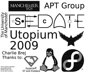
And then you’re done. The Utopium logo looks like this. Make sure you get permission to use any copyrighted artwork or trademarked designs (I did, thanks Fedora for letting me use your logo).
